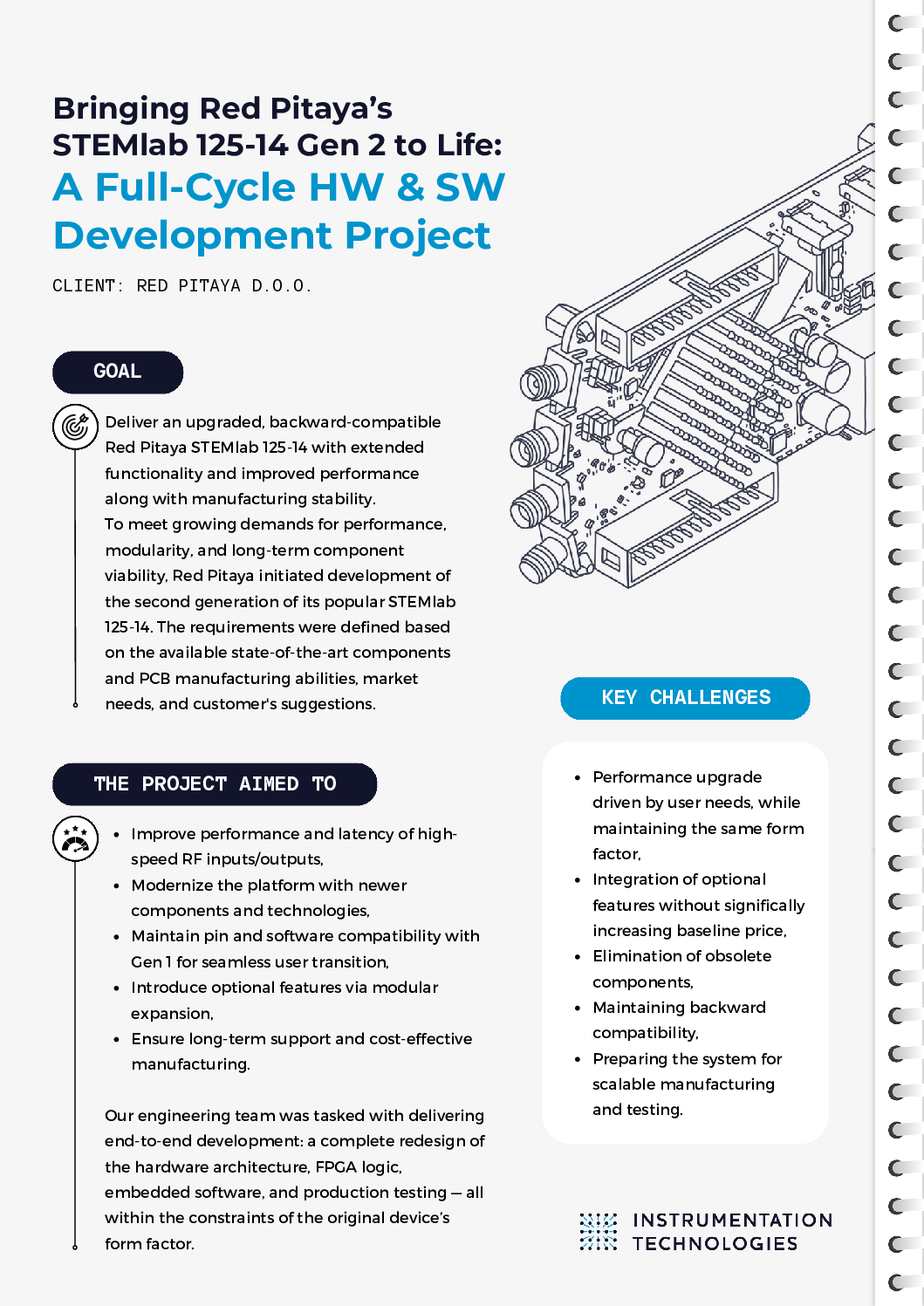
A full-cycle hardware and software developement project completed in 12 months.
Bringing Red Pitaya’s STEMlab 125-14 Gen 2 to Life
To meet growing demands for performance, modularity, and long-term component viability, Red Pitaya initiated development of the second generation of its popular STEMlab 125-14.
The requirements were defined based on the available state-of-the-art components and PCB manufacturing abilities, market needs, and customer’s suggestions.
THE PROJECT AIMED TO:
- Improve performance and latency of high-speed RF inputs/outputs
- Modernize the platform with newer components and technologies
- Maintain pin and software compatibility with Gen 1 for seamless user transition
- Introduce optional features via modular expansion
- Ensure long-term support and cost-effective manufacturing
Our engineering team was tasked with delivering end-to-end development all within the constraints of the original device’s form factor:
KEY CHALLENGES
- Performance upgrade driven by user needs, while maintaining the same form factor
- Integration of optional features without significally increasing baseline price
- Elimination of obsolete components
- Maintaining backward compatibility
- Preparing the system for scalable manufacturing and testing
OUR APPROACH
1. Collaborative Specification & Planning: Together with Red Pitaya’s R&D, we consolidated feature requests from the user community and mapped them into a structured development plan.
- Feature classification: Mandatory vs. Optional
- Optional features implemented on add-on board to enable price segmentation
- Weekly development reviews enabled rapid feedback and alignment
2. Full Redesign of HW & SW: We replaced and redesigned all major subsystems.
- Hardware: Front-ends, clocking, RAM, power supplies
- New multi-purpose connector for modular add-ons (8x high-speed differential pairs)
- High-Density Interconnect (HDI) PCB and integrated power supplies to maximize board space real estate
3. FPGA & Embedded System Improvements:
- eMMC boot support added via new Linux U-Boot config for boot image loading over add-on boards
- Added frequency counter for better diagnostic insight into ADC clocks
- New FPGA tests to validate high-speed differential links (250 MHz serial + clock pairs)
- Internal FPGA constraints to optimize signal timing
4. Validation & Test Strategy
- Each major hardware update verified on evaluation platforms before integration
- System-level testing ensured performance stability across all functions
- Full manufacturing test framework prepared to scale production confidently
- Longevity and availability of all components validated
OUTCOME
STEMlab 125-14 Gen 2 now offers:
- Noise and impedance improvements with lower timing latency in high-speed interfaces
- Internal/external clock selection
- An additional E3 connector to extend boot possibilities with eMMC, QSPI, WDuC, and to access high-speed lines
- Modernized architecture without disrupting existing users
- Clear modular functionality upgrade options for extended use cases
- Improved diagnostics and configurability
- Manufacturing-readiness with validated BOM and production testing
CONCLUSION
The project was completed in line with initial time estimates (approx. 12 months), thanks to joint planning, agile iterations, and tight technical collaboration between both teams.
This project illustrates our ability to take on complex, multi-disciplinary engineering projects – integrating hardware design, FPGA development, embedded systems, and testing. Whether working with external customers or internal product teams, our development approach ensures transparency, adaptability, and long-term product viability.
Services
Others Also Looked
Product Development
Product Development
We understand that bringing a new product to market can be a time-consuming process. For that reason, we provide our…
Design Consulting
Design Consulting
Being familiar with technological possibilities and limitations, knowing how to create the best possible design to achieve the results required,…